|
Z80 Build From Scratch |
| PAGE 8: Testing RAM |
|
Question: We tested ROM by setting all of the data to 0x00, NOPs, which meant the system would do nothing but advance to the next memory location. But how would we test the SRAM? Answer: We could write a small program in machine language and burn it to the FlashROM.
Z80 has some very powerful
instructions and one of our faves is LDIR. The ldir (Load,
Increment, Repeat) instruction in the Z80 microprocessor copies
a block of memory from a source address to a destination address.
It performs this by reading a byte from the address in the HL register
pair, writing it to the address in the DE register
pair, and then incrementing both
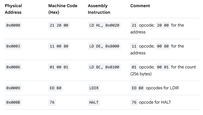
For our code we'll write the code at position 0x0000 in the ROM. At location 0x20 we'll write an alternating pattern of FF then 00 for a total of 16 bytes. We want to copy it from the ROM to the RAM which starts at location 0x8000. The source address in the HL register pair will be 0x0020. The destination address in the DE pair will be 0x8000. Register pair BC will contain the number of bytes to copy which is 0x0010. Z80 Assembly Code
When this assembly code is assembled into machine code, some changes will be made. For example, Z80 like many CPUs of its era use Little Endian Byte Ordering: the low byte is placed in the memory location first followed by the high byte. So the address 0x8000 would have 00 in the first address location and 80 in the second address location. Here is the machine code: Z80 Machine Code
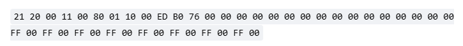
The final sequence of bytes we would manually input to the ROM starting at address 0x0000 are:
But we also need the data to display as alternating bytes of FF and 00, starting at location 0x0020 so the final code would look like this:
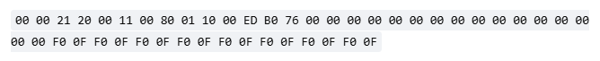
On second thought, we'll use "F0 0F" instead because we can see the data alternately flashing on the left then right side of the LED bar graph. Additionally, a zero does not light up an LED so we won't know which address we're currently working on. A better choice would be to start the code at address 0x0002. We can do that by adding two NOPs (0x00) starting at address 0x0000. So let's use:
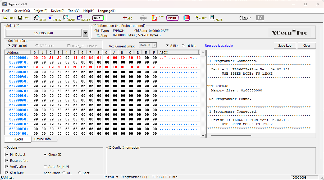
If we start up the ROM programmer, this is what we will flash to the ROM:
When you're done don't forget to hit File then Save, save as .\Xgpro\UserData\SST39SF040\Test_RAM.bin.
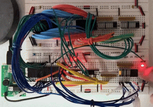
One-Minute Video of RAM Test from Boot
(Click to enlarge) In the video you can see the "F0" (1111 0000) flash at about 22s in. Just prior to it at address 0x000B is instruction ED (1110 1101) and at address 0x000C is instruction B0 (1011 0000).
|

![]()
Updated 2025-11-27