|
Z80 Build From Scratch |
| PAGE 7: Adding Addressing Logic |
|
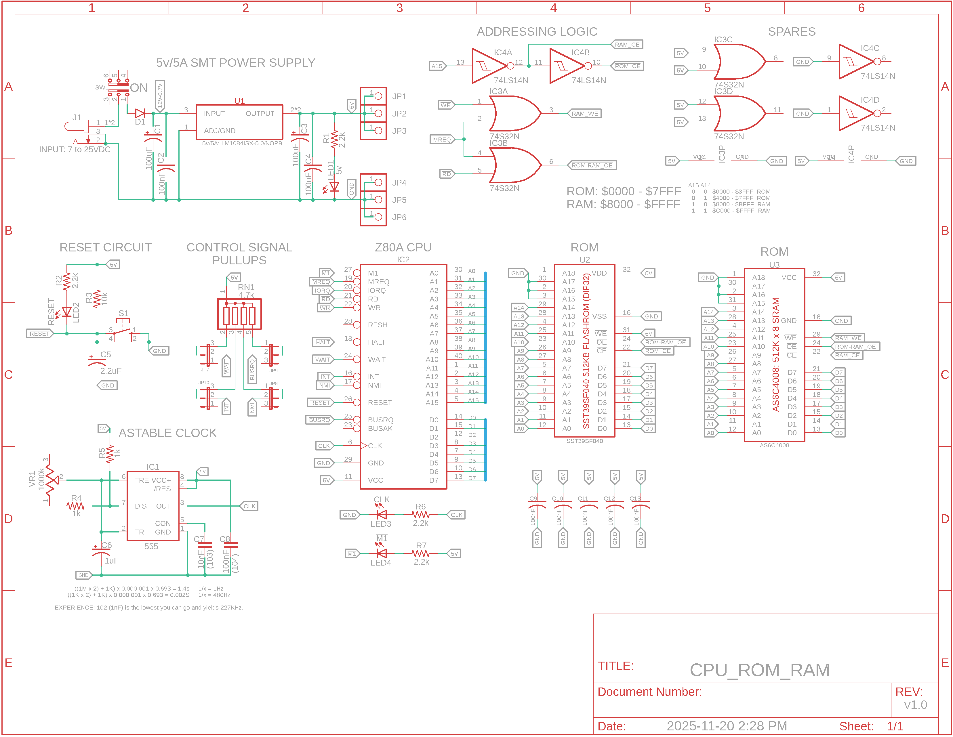
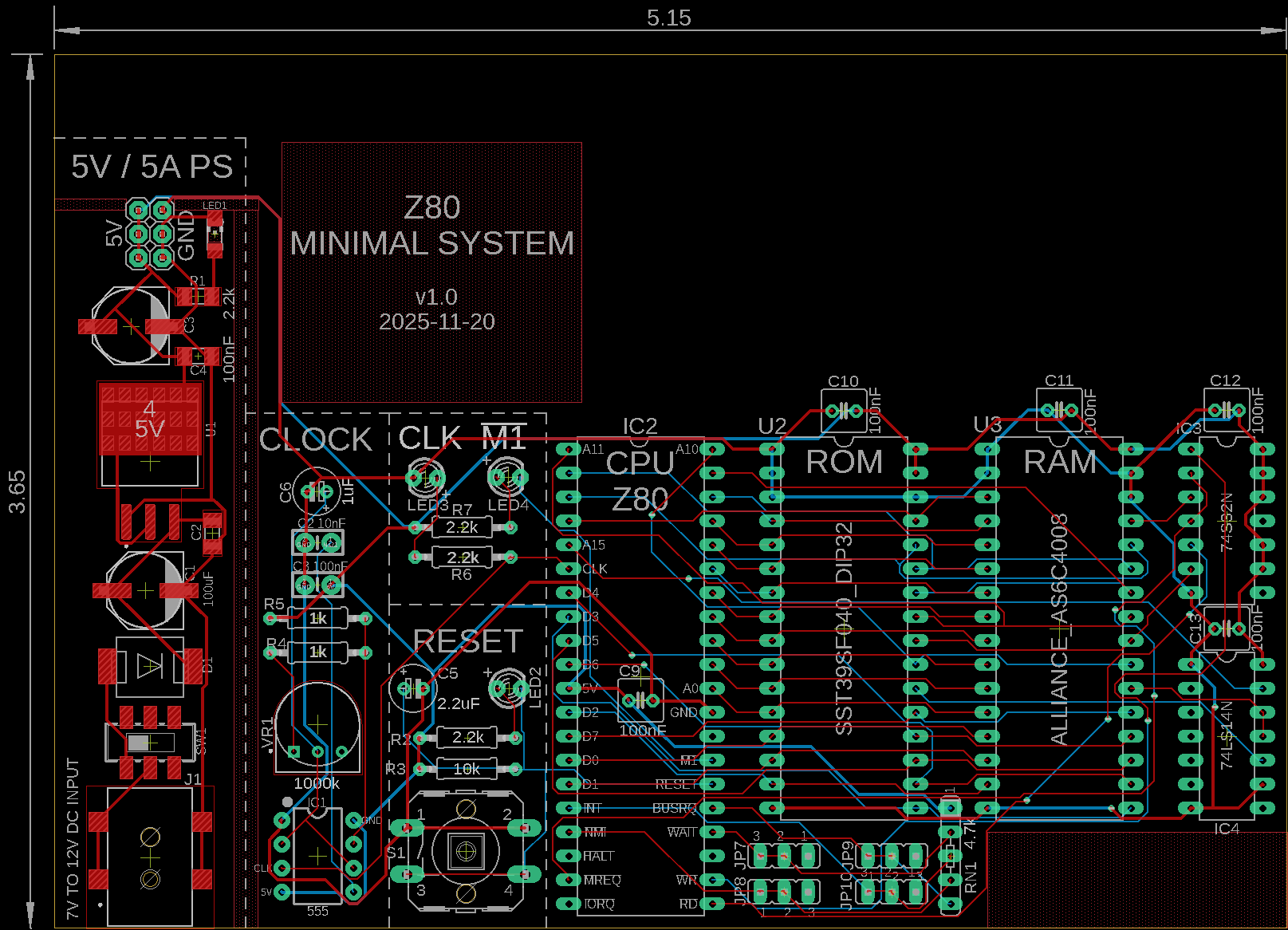
Let's apply our revised design to a schematic and board layout. The LED bar graphs have been removed. The ROM and RAM have been added to the design as have the two logic devices, an OR device and a NOT (inverter) device. You may have noticed the 4 unused control signals are still pulled up to 5v via termination resistors but there's also a jumper on each so they can be routed to some other part of the board if needed.
Schematic, Board Layout, PCB
(Click to enlarge)
By default, new ROMs are configured with each location containing 0xFF which as a Z80 instruction performs a "RST 38H". This will force a jump to location 0x38 looking for an interrupt service routine which does not exist yet, and it will probably cause the program counter (PC) stack overflow as the current address is added to the small stack. Either situation is not good so I used the chip programmer to zero out the ROM. Zeroes (0x00) when read as Z80 instructions are NOPs (no operation) which increment the program counter and address to the next location. We can use that to see if our system is working as the addresses march from 0x0000 to 0xFFFF.
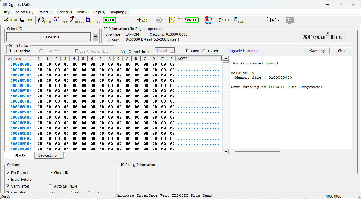
Burning Your First ROM: - Open the Xgpro v12.60 app - Place your chip in the very top of the ZIP socket, oriented with the chip cutout at the top near the vertical lever - Close the lever so that the chip does not move within the socket. You should wiggle it back and forth to ensure good contact. This won't be the last time you'll do this as you'll see - Within the app, click the large Select IC button - In the Search Device box, type the specific chip name. In my case it's SST38SF040 - Four selections will appear. Only the first one does not have a packaging variant like PLCC32. Highlight and select it - You should see a grid of FF bytes which is the default configuration data for all new ROMs - Right-click within the grid, preferably to the right in the ASCII section where there is nothing but periods - Choose Fill Block/Swap(F); a form will appear. In the Format section you should see FF as the Value(Hex). Change it to 00 - To the right is a button labeled FILL: click it. All of the hex data should change from FF to 00. Click the Back button - You're now ready to program the chip. In the top middle is a button that reads PROG. Click it followed by the Program button. Ignore the error about no buffer loaded by clicking OK - The programming should take less than a minute - If you get a programming error and the adjacent diagram of the chip in the ZIF40 socket has a little red X beside any of the pins, release the socket lever, wiggle the chip, and then set the socket lever. You may have so do this a few times to improve the electrical contact. When done, click BACK - All of the data should now be zeroes. You're done! Xgpro v12.60: TL866II Plus Programmer
(Click to enlarge)
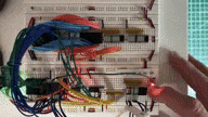
The system was built on a breadboard using the schematic at the top of this page. ROM and RAM were added to our system. A red LED was attached to A15 such that when it went low, the LED illuminated. This tells us we're working with ROM instructions. The Flash ROM was programmed with nothing but 0x00 to ensure the Z80 CPU would read them as NOPs and do nothing but increment the Program Counter which in turn will increment the address from 0x0000 to 0x0001 and onwards. A LED bar graph was attached to the address range of A7 to A0 on the RAM because it was more easily accessible. It's the same pinout on both the ROM and RAM. The system was reset by holding down the Reset button for at least 3 ticks of the clock. The control signals of M1, MREQ and RD illuminated for each memory read as we expected them to. The binary addresses shown in the bar LED graph proceeded from 0000 0000b to 0100 0101b (0x45) when the video ended.
Video: Test ROM Operation
(Click to enlarge)
|

![]()
Updated 2025-11-27