|
Z80 Build From Scratch |
| PAGE 6: Adding ROM and RAM |
|
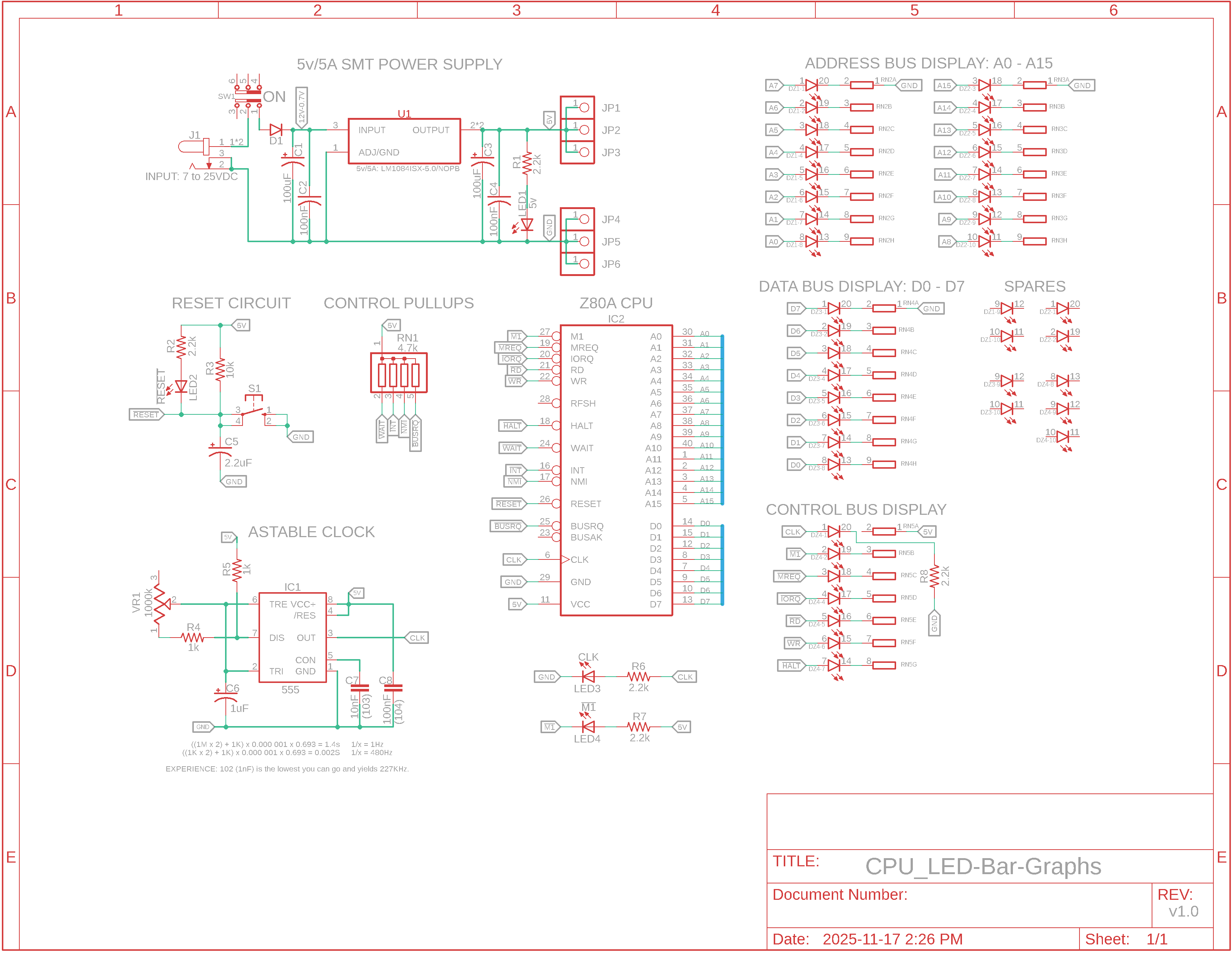
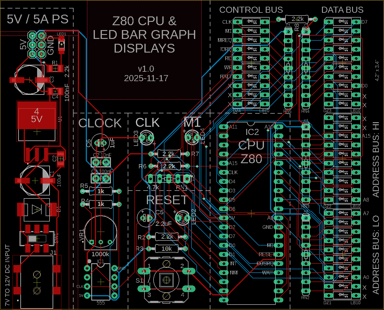
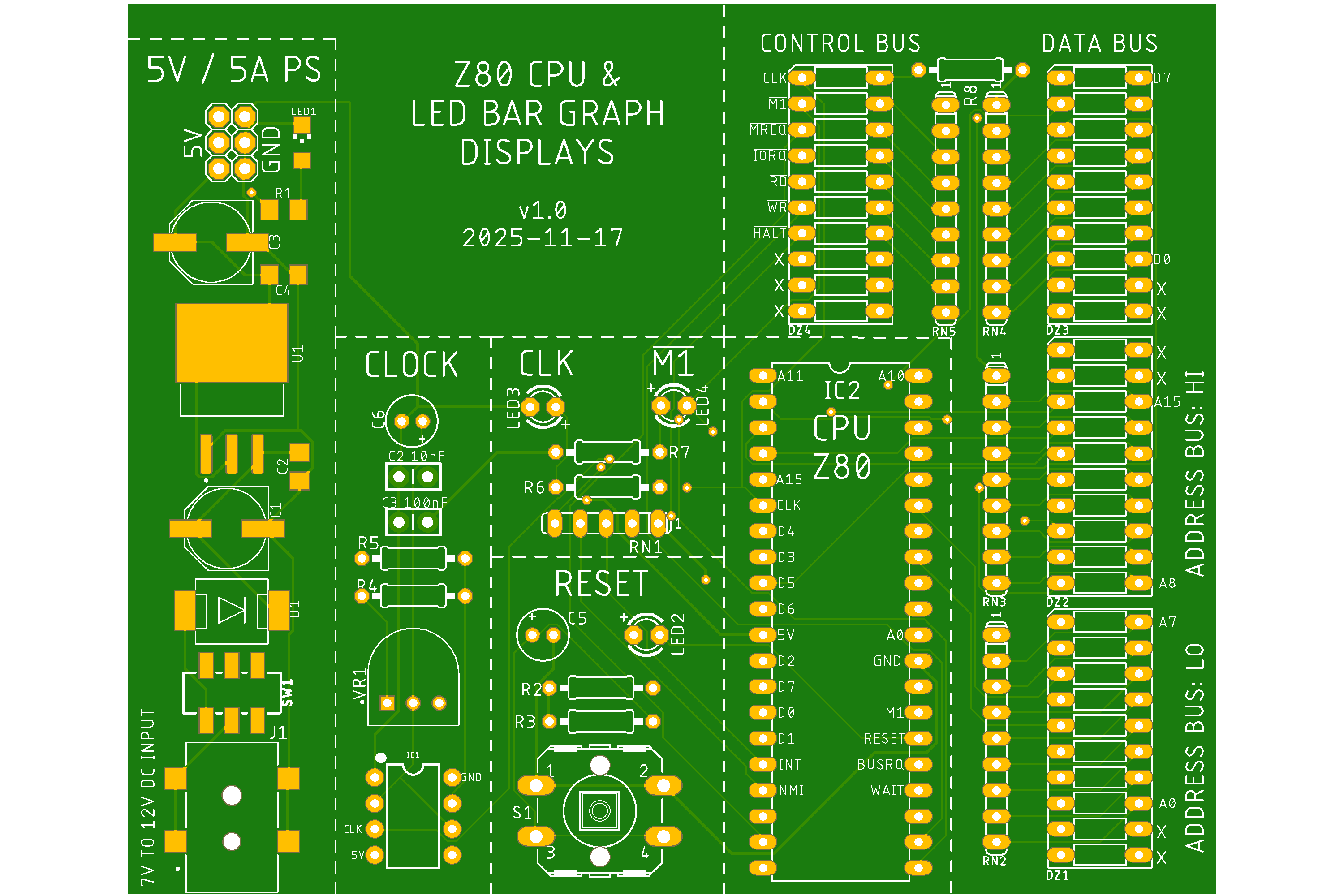
If we designed a PCB using Eagle CAD v9.6.2, what would it look like? Schematic, Board Layout, PCB
(Click to enlarge)
We say this is faking a system because we know what it looks like, we can order the PCB via the Eagle gerber files from JLCPCB.com, we can then populate and test it, but all it does is count to the maximum binary value that will be shown in the LED bar graphs and nothing else. We need to replace the displays and their resistors with a ROM that contains real instructions of what we would like the Z80 CPU to do.
Ben Eater has several good videos related to EEPROMs and building an EEPROM programmer using an Arduino Nano. I followed his great directions and built one which I used for about six months until I realized it was taking me a lot longer than I cared for to get the growing program and its routines into the ROM. I finally decided to buy a professional EEPROM programmer, write the assembly code mnemonics (not machine code) in an editor, assemble it into a hex file of machine code and then use the programmer to quickly write it to the ROM.
That means we need to update our schematic to include a ROM. There are several EEPROMs available as Flash ROMs. Initially I'm going to use an SST39SF010A in a 32-pin DIP package and later I'll switch to using the much smaller SST39SF010A in a PLC22 package.
We can add ROM and RAM chips, hook up the address and data lines but we'll have to figure out which addresses to use. As you saw in the video on the previous page the Z80 starts counting at address 0x0000 after being reset so that would be a good place to put our permanent instructions that we'll store in a Flash ROM. If we use 32KB ICs we can use the first 32KB in the memory map for ROM and the second 32KB for RAM. The starting value for ROM we said would be 0 (0x0000) and the ending value would be 32,768 - 1 or 32,767. In hexadecimal that would be 0x7FFF. If we were to structure the addressing so the RAM starts immediate afterwards in our basic memory map, then the RAM addresses would be 0x8000 (32,768) to 0xFFFF (65,535) for a total of 64KB.
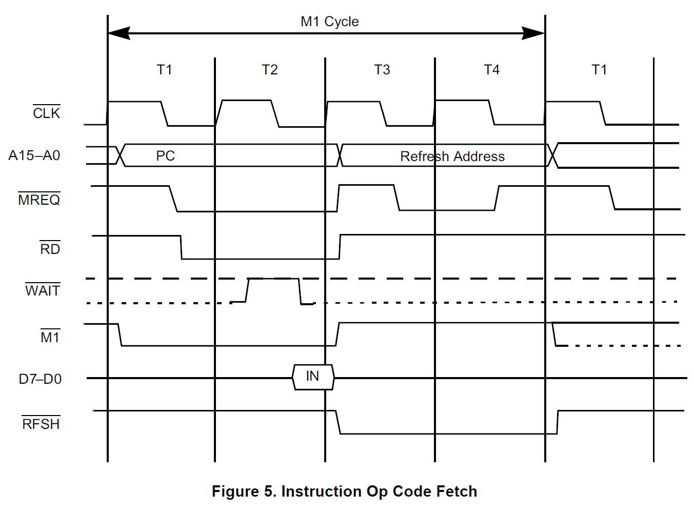
Looking at page 9 of the Z80 User Manual you can see the Instruction Op Code Fetch process in Figure 5. When M1 goes low on the first clock tick it is followed by MREQ and RD together. You can see that in the video, too. (Those LED resistors are tied high so a low illuminates them.) If you examine Figure 6 on page 10 of the user manual, you'll see that MREQ will be low when WR is asserted, too. So our address selection scheme needs to include these.
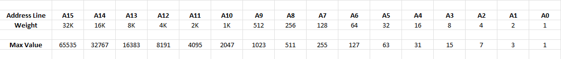
The table below shows the address line weighting. The only two address values we will see on just the A0 line are 0 and 1, so A0 has a weight of 1. On A2 it's 2. On A3 it's 4. On A8 the weighting is 256 and on A15 the weighting is 32K. If we populate all of the addresses from A14 to A0 with ones, the Max Value will be 32,767 or about 32K. From the table below you can see that from an address selection process, A15 represents 32K. If no other line is used and A15 is a 0 then the address is 0. If no other line is used and A15 is a 1 then the address is 32k. So we can use the A15 line to choose our ROM or RAM devices: A15 = 0 is ROM and A15 = 1 is RAM. This greatly simplifies our design.
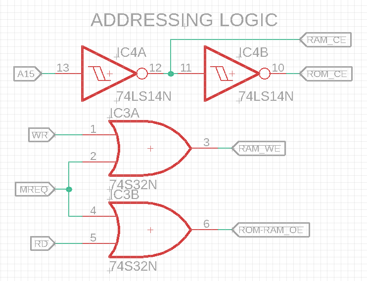
In the Memory Addressing Logic schematic below we can can see the addressing choice in the top part (IC4) and the control logic (IC3) below it. If you put a 0 on A15, that low will propagate through as a 0 until it hits the first inverter, gate IC4A, where it will become a 1 at pin 12. Going thru the second inverter gate (IC4B) at pin 11 changes it back to a 0. So A15 will be our ROM Chip Enable line going to CE on the ROM because it selects the lower 32K when it's a zero. When A15 is a 1 it is inverted to a 0 as it exits gate IC4A and goes on as RAM_CE to CE on the RAM chip to enable the RAM. The ROM will not be enabled. Our addressing is complete: A15 low is ROM and A15 high is RAM.
Control logic: with MREQ low and either RD or WR also low (they cannot both be simultaneously selected: you are reading or writing), the output of both memory devices (ROM or RAM) are enabled via ROM-RAM_OE but only the one with the current CE line also selected will be engaged.
|
![]()
Updated 2025-11-27