|
Z80 Build From Scratch |
| PAGE 5: Address Testing |
|
Intro: One of the Z80 instructions we will start with is the NOP or No OPeration (page 180 of UM0080.pdf) which has a numeric value of 0x00 (hexadecimal zero). It does nothing but buy time. There will be situations where we can use that to our advantage. You will find it in the upper left corner of Z80_CPU_Microprocessor_Instant_Reference_Card.jpg. It's the intersection of 0 and 0 of the grid.
Using NOPs as data: The address bus starts at location 0x0000 when the system is rebooted. If we were to place a NOP instruction on the data bus at this address location of zero, the address bus will read it in, execute it and advance the program counter (PC) to the next location, 0x0001. If we tie the data bus to ground then it will always read 0x00 as the data at any address location. So after 0x00 is read at location 0x0000, the PC will increment to 0x0001 and the address bus will read the data from that location. Thanks to the data bus being tied to ground it will read another 0x00 and do nothing except increment the PC which will point the address bus to location 0x0002. This will continue until it hits the maximum of its 64KB address range and then start over at 0x0000.
Warning: Should we tie the data bus to zero? If we are outputting a zero - no harm. However, if the system received a non-zero value that it may try to write to the data bus, that will cause a short circuit. The CPU may survive but you can bet it will heat up quickly and most likely fail. So to prevent that, for our experiment we'll tie all 8 lines, D0 to D7, of the data bus to ground but through 4.7k resistors or a 4.7k "SIP pack".
Resetting the CPU: We can use a resistor and LED combination for the reset LED but that takes up more breadboard (BB) real estate. Or you can use the LED and 2.2k resistor device you may have made earlier on page 2. Attach the insulated lead to the RESET pin and the resistor lead to 5v. When we hold down the reset switch for 3 clock ticks, we can see the LED illuminate thanks to its path to ground via the RESET pin.
Displaying Addresses: If we attach a 4.7k resistor to an LED, it may not illuminate at all. I have tried 2.2k resistors and they have worked OK. They're not very bright but when it comes to taking a picture of them, they don't overwhelm the display. If we want to see the address being output on the address bus we can use LEDs. 4.7k resistors won't work but 2.2k resistors will. Do they represent an increased load to the CPU? Yes, but we are running at very slow speeds so we should be able to use them briefly without incident. Place your finger on the CPU while it's running and you'll know if it's overheating.
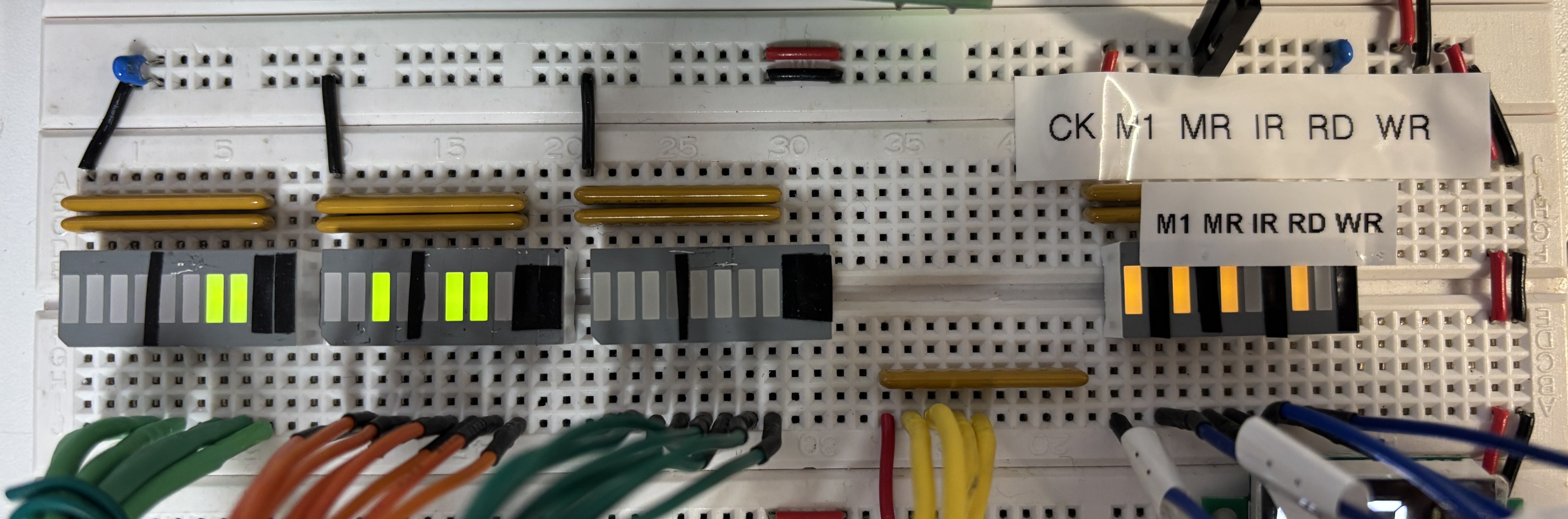
Connecting LED Bar Graphs: The address bus is 16 pins, the data bus is 8 pins and the usable control bus signals are 6 pins. That's a lot of LEDs taking over your BB! What we could use instead are LED Bar Graphs. We would need 4 of them and 4 resistor packs. Below is a photo of all 4 graphs connected to the CPU (not shown). The two left-most devices are for the address bus with A15 to A8 on the left and A7 to A0 on the right. The next device to their right is the data bus with D7 on the left and D0 on the right. Notice how no LEDs are lit on this bar graph. Much further right are some of the control bus activity signals: CLK, M1, MREQ, IORQ, RD and WR. You'll notice that each LED bar has two resistor SIPs attached to it. That's because I ran out of 2.2k ohm SIPs so I decided to use two 4.7k ones in parallel. In series you add the resistance but in parallel you divide the resistance so it's about 2.35k ohms. It's good enough for these LEDs because you can see them lit in the photo below. Something else you may notice is that these are 10-LED graphs, not 8-LED graphs. Subsequently, some of the LEDs have been taped over. Also, there are black separator between each 4 bits to make them easier to read.
LED Bar Graphs: Address Bus High and Low (2), Data Bus (1), Control Bus (1)
(Click to enlarge)
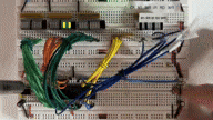
Action Video: (Note: you may be able to reduce the playback speed to 0.25x in the vertical "..." elipse menu for the video below.) In the video below the reset switch in the lower right corner is held down for 3 ticks of the CK (Clock) LED in the Control Bus LED bar graph in the top right. Then we see the following: - the clock (CK) LED ticks in the Control Bus LED Bar Graph in the upper right part of the screen - the user withdraws his finger from the reset switch after watching the CK LED tick 3 times: the CPU is restarting at address 0x0000 - M1 LED illuminates and starts an M1 cycle by lighting MR (Memory Request) and RD (Read). There is an additional tick where MR lights again but that's to finish the last read - once those LEDs extinguish, a new M1 cycle starts and we see an LED illuminate in the A0 (right-most) position of the Address bar graph - the process continues to repeat - in the lower left corner of the video the user is using a screwdriver on the variable resistor (potentiometer) to increase the clock rate - you can see the LEDs count upwards in binary until the count approaches 0000 0111 1011 1111 or almost 0x07FF on its way to 0xFFFF - at that time the one-minute video was terminated
Video: Address Bus Counting from Zero
(Click to enlarge)
|
![]()
Updated 2025-11-27