|
Z80 Build From Scratch |
| PAGE 4: Connecting Circuits |
|
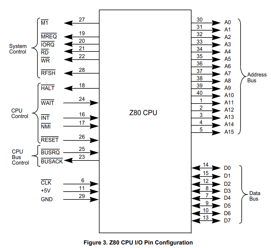
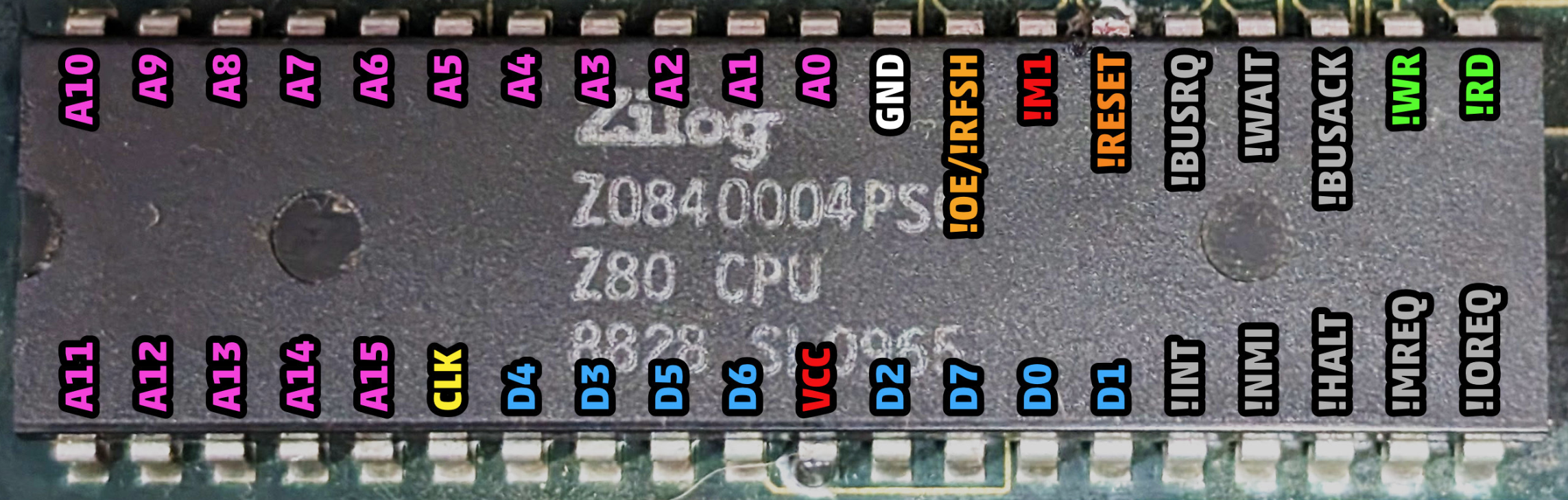
Z80 Logical and Physical Pinouts
(Click to enlarge) Let's Briefly Examine Z80 Signal Blocks: Address: A0 to A15 Data: D0 to D7 System Control: M1, MREQ, IORQ, RD, WR CPU Control: HALT, WAIT, INT, NMI, RESET, BUSRQ
We should pull up some of the unused Control Signals to 5v but through 4.7K resistors. We'll use a bussed resistor network SIP pack: pin 1 goes to 5v and the remaining 4 pins go to the 4 control signals (WAIT, INT, NMI, BUSRQ) on the CPU.
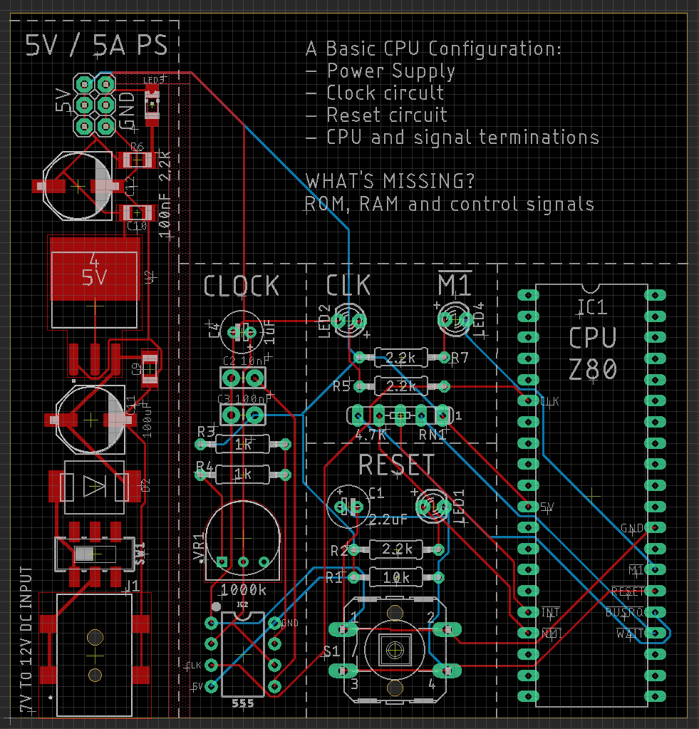
A Starting Schematic: Below is an Eagle v9.6.2 schematic that illustrates the circuits we have built so far: - At the top of the schematic diagram the 5v power supply could be the narrow breadboard rail ps shown attached or it could be a 5v phone charger - We can see the clock circuit we built in the lower left using a 1M ohm variable resistor and 1uF electrolytic capacitor for a clock rate of 1Hz to at least 100Hz - Above the clock is the reset circuit. The LED will only illuminate if the momentary switch is pushed which gives the LED circuit a path to ground. Note that the switch must be held for 3 ticks of the clock or the CPU will not recognize it as a reset signal - Next to the reset circuit is the 5-pin 4.7k ohm bussed resistor network SIP pack that we will tie the unused control signals to so they won't float and mess with our system - And finally on the right is our CPU showing all of its current connections
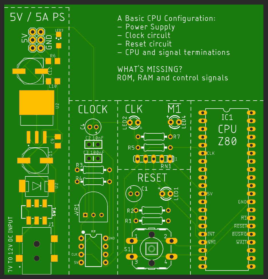
A Starting Board Configuration: To the right of the schematic is the PCB board showing how we might layout the circuits. The potential printed circuit board (PCB) is show right-most below. Nothing is attached yet to the address and data lines as well as their respective control lines.
Next: We'll "fake" ROM and RAM as part of our understanding of CPU input and output.
|

![]()
Updated 2025-11-27