|
Z180 Single Board Computer |
| PCB Circuit (click to enlarge) | Z180 SBC Circuits and Info |
|
Z80 Functional Block Diagram
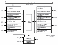
Asynchronous Serial Communication Interface (ASCI) Block Diagram
Eagle CAD: 3. _________
Control/Status Register S1
Adafruit DS1307 RTC Breakout Board
BOM (Bill of Materials) |
Hardware Reference: In addition to all of Z80's functionality, the Z80180 a.k.a. Z180 also has several features including built-in functions of other chip devices: - full Z80 compatibility as well as extended Z80 instructions - 2 UARTs - 2 16-bit counter/timers - on-chip oscillator/generator - on-chip interrupt controllers (INT0, INT1, INT2) - expanded memory management unit (MMU) addressing up to 1MB (512KB with 64-pin DIP) - 2 DMA channels - 3 on-chip wait-state generators - HALT, SLEEP, and low-power operating modes - clocked serial I/O port - 3 packages: 64-pin DIP (no A19 pin), 68-pin PLCC, 80-pin QFP How do the Z80 and Z180 pinouts differ? - Input EXTAL replaces CLK and is Schmitt-triggered - Output PHI is a clock signal at one-half the speed of EXTAL - UART0 has full modem control but UART1 does not so control signals will be missing - CKA0 & CKA1: Tx and Rx clock outputs from the ASCI baud rate generator, or as external clock inputs for the same - CKS is the clock for the CSIO clocked serial I/O channel, TRDR is for control, TXS and RXS are transmitted and received data for the channel. See page 14 of the Z180 manual - etc.
Internal Registers The Z180 has several new features like dual UARTS, etc. Each function requires its own registers; this is the list of Z180 registers you will want to add to your code.
Internal Registers Reassignment The register numbers start at 0x00 which may interfere with devices that you may wish to add to your design. The Z180 relocate internal registers.asm file provides you with the commands needed to change the default I/O location to other 0x40 blocks.
How do I test the P-to-I2C? Z80 assembly file: _______
I see the schematics. Where is the Bill of Materials parts list? Here is a link to _______
Note: M62 Bus is copyrighted by Peter Murray of Murray Electronics, http://www.39k.ca |
