|
ZB64EC-bus Z80 MBC System |
| PCB Circuit (click to enlarge) | Circuits and Info |
|
The ZB64EC-bus Z80 is a multi-board modular system; it is not a single board computer like the M62-bus and ZB64PC-bus based systems. |
|
|
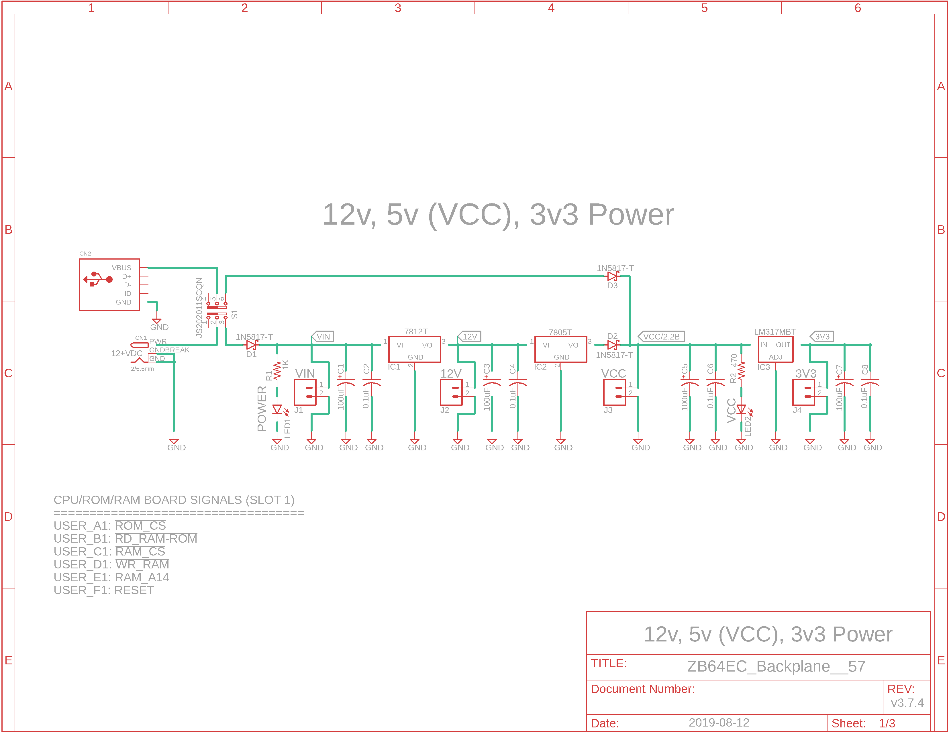
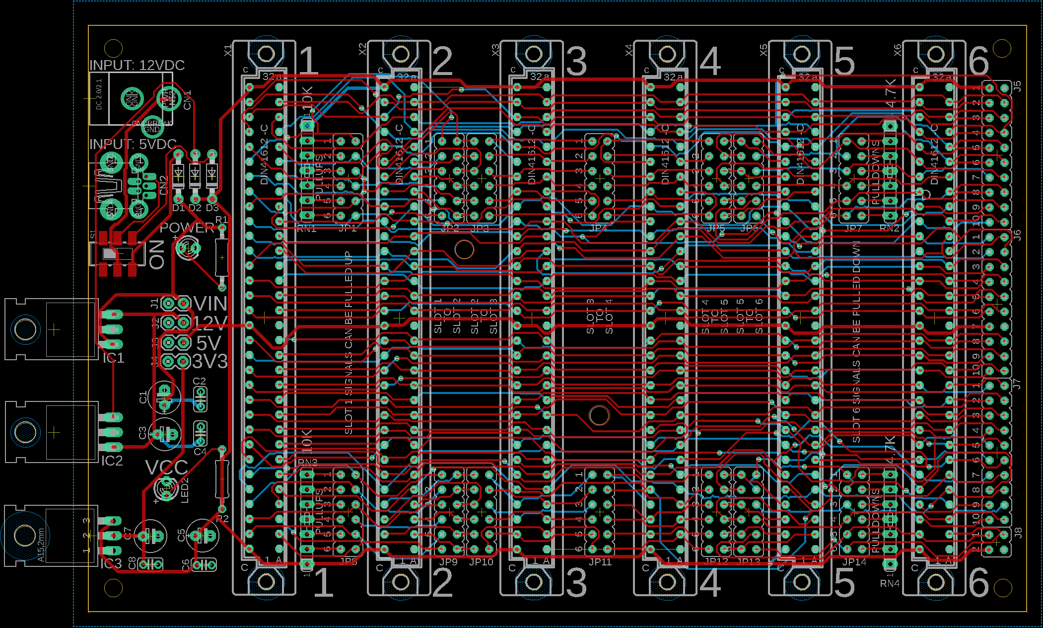
Eagle CAD: 0. Powered 6-slot Backplane
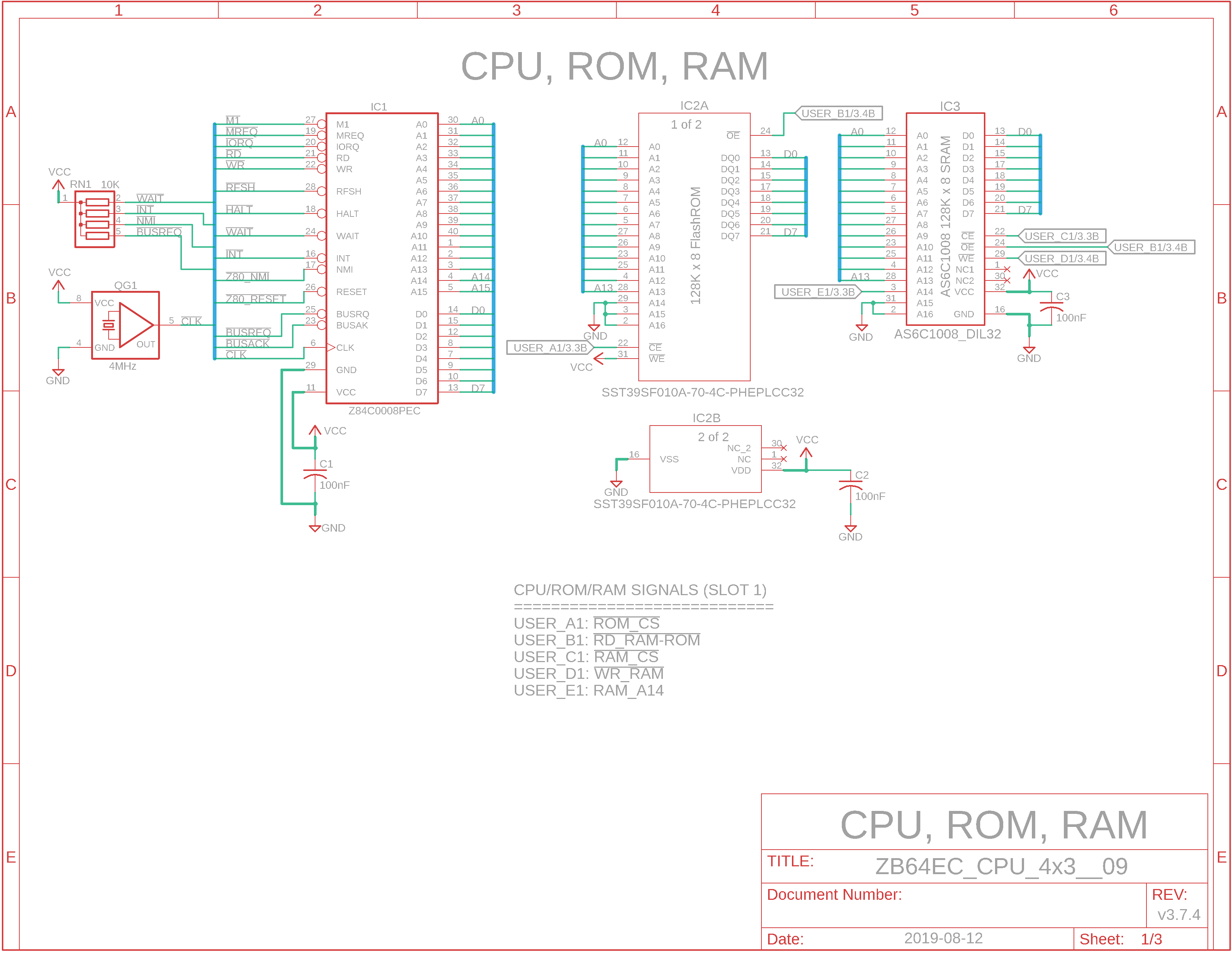
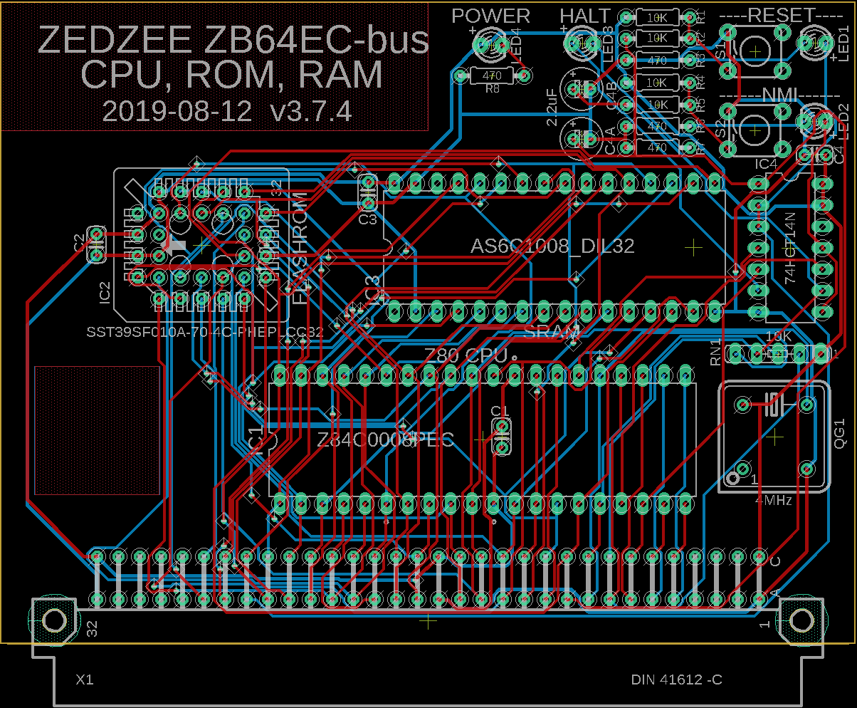
Eagle CAD: 1. CPU, ROM, RAM
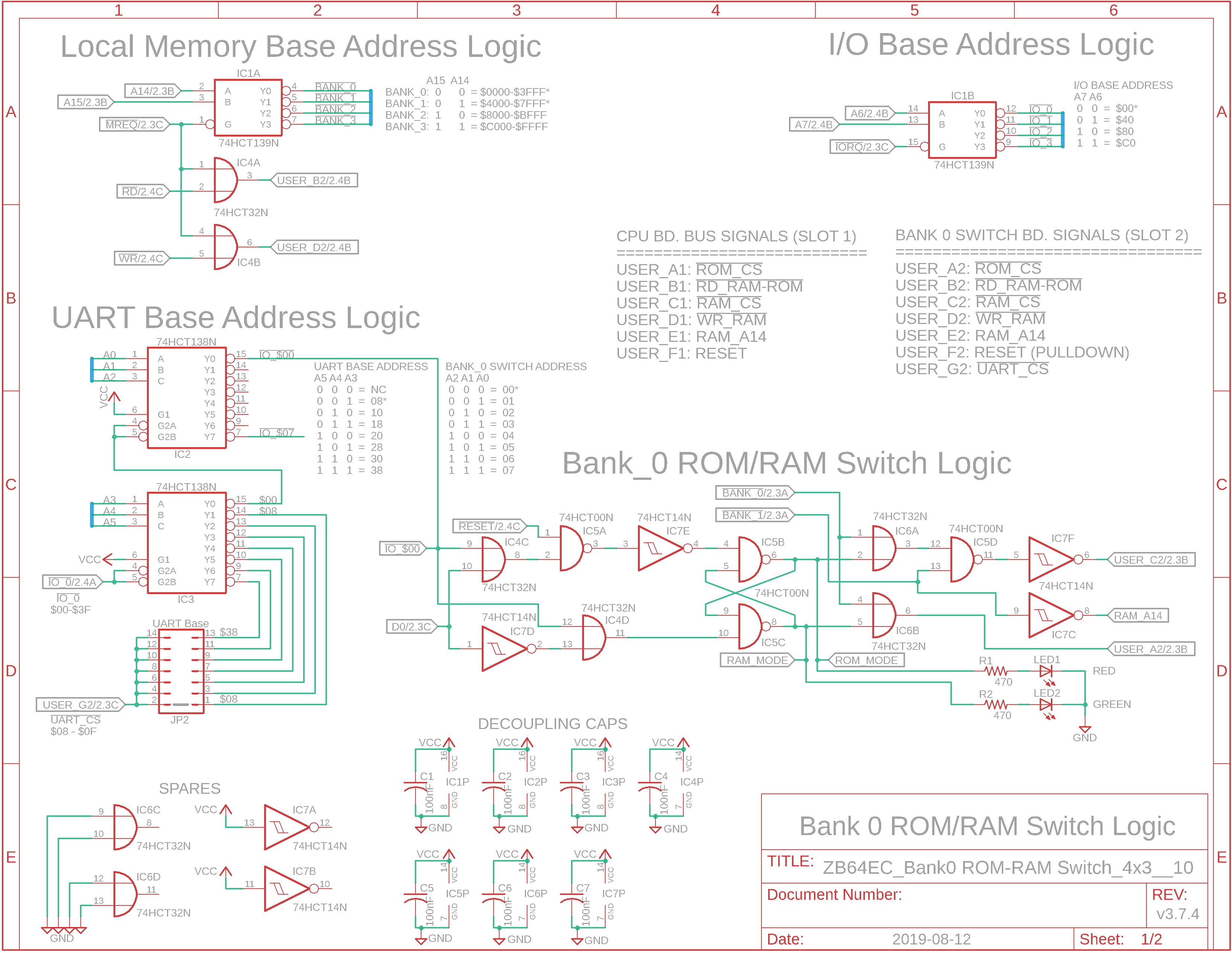
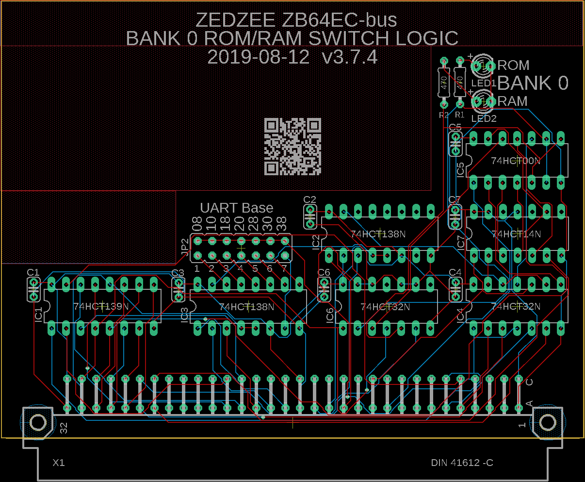
Eagle CAD: 2. Memory Bank 0 ROM/RAM Switch
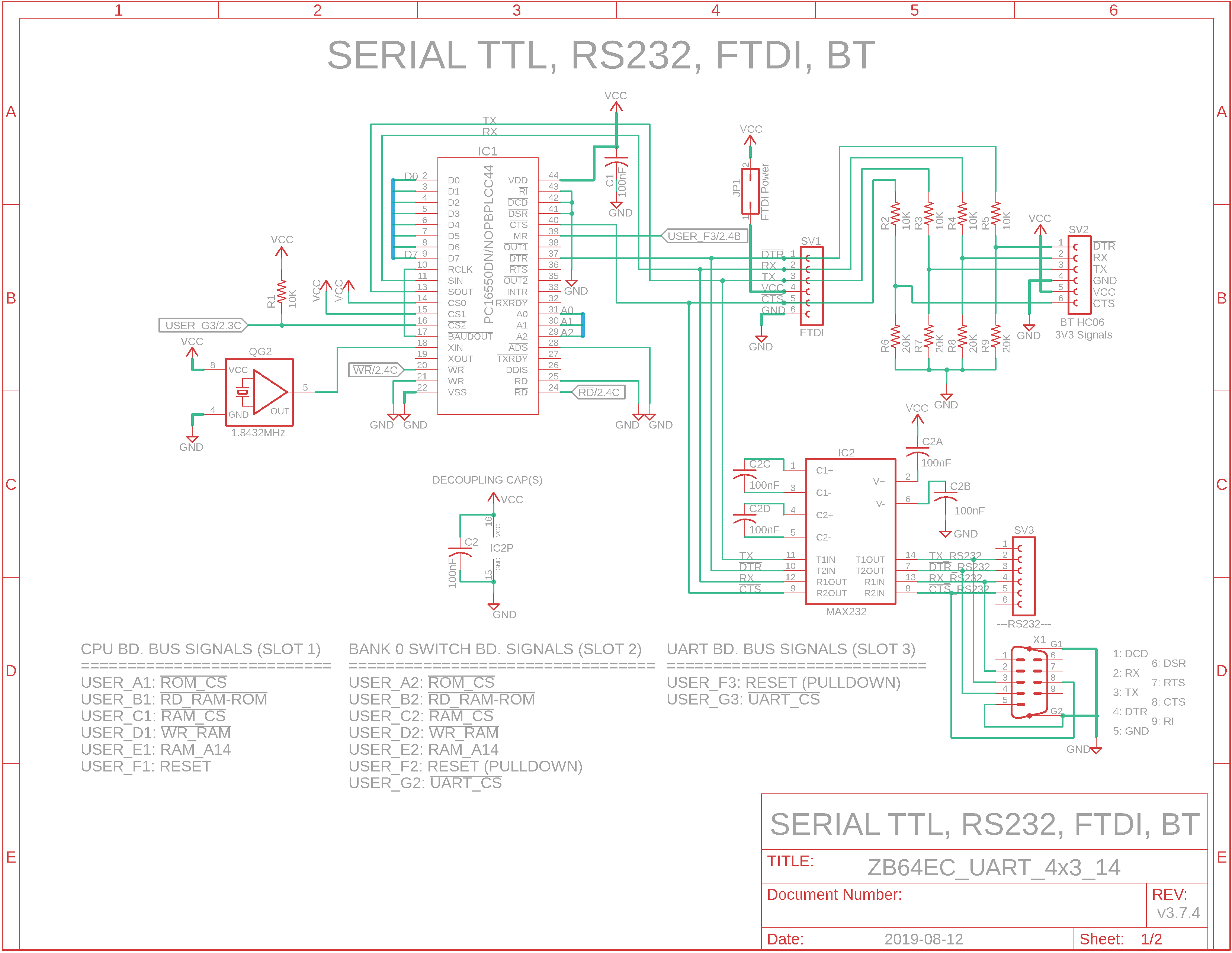
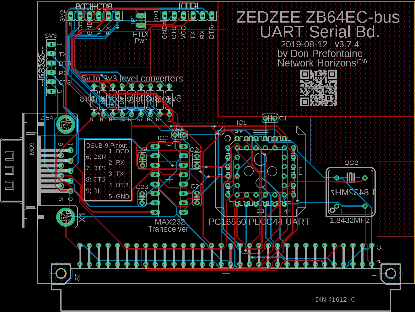
Eagle CAD: 3. UART, USB/FTDI, Bluetooth, RS232
|
System Overview The basic system is modular and is composed of 4 boards: - an extendable 6-slot backplane - a CPU/ROM/RAM board - a Bank0 ROM-RAM switch board: permits the unused memory in the lower 16KB part of ROM to be used as RAM - a UART board for terminal communcation: USB/FTDI, RS232/Bluetooth, and RS232 D-sub
Additional boards can be added to the system, including a bus extension board. See the ZB64EC-bus Z80 MBC menu for the current list.
System Features 1) Essential system functions have been distributed over 3 boards. The boards are 4" wide x 3" high (102 x 76mm). This makes for easier troubleshooting as well as learning how the system and bus communication works. 2) 12 user bus lines, USER_A to USER_L, have been added for customization. These are in addition to the BANK_0 to BANK_3 and IO_0 to IO_3 bus lines created by Peter Murray of 39k.ca for his M62-bus based Z80 SBC. Each USER_x bus line can be terminated high (10K) or low (4.7K) or not at all. 3) Each bus line is available at each slot via jumpers. It is possible to use a single bus line across the backplane many times for different functions. 4) You can design your own boards to add them to the system, and use any of the available bus lines or bus line sections.
The Bank0 ROM RAM switch board explained With many existing ROM monitors or BIOSs, only a portion of the ROM is used which essentially results in memory waste. Peter Murray engineered the idea of making use of the unused memory. If the Z80 64KB memory is carved up into four 16KB banks, the first 16KB (BANK_0) is typically used for ROM. The next 16KB (BANK_1) is used for RAM, as could be the remaining two 16KB banks. (However as you will see with the Memory Expansion Board, RAM MEB, we'll set aside the 16KB BANK_2 to be used as a window into many, many 16KB banks of RAM. The same could also be done with a ROM MEB. More on that later.) If we copy the small ROM Monitor/ROM BIOS of BANK_0 into the RAM of BANK_1, then switch BANK_0 to be used as RAM, we have recycled a "lot" of RAM that would otherwise go untapped.
How is the bank switching done? If you examine the adjacent screenshot, Eagle CAD: 2. Memory Bank 0 ROM/RAM Switch, in the right-middle you'll see that IO_0 (I/O addresses $00 to $3F) and I/O address $00 (default) will set Bank 0 to be ROM. If however, if you write value $01 instead of value $00 to address $00, the system will enable the RAM_A14 line (carried from the switch board to the CPU board via USER_E1 and USER_E2 jumpered with JP1 and JP2 on the backplane). That means the lower 16KB of this 128KB chip will be used as RAM BANK_0 and so will the next 16KB as RAM BANK_1. (The remaining RAM has its address lines above A15 tied to ground so they aren't used.) The lower right portion of the schematic also shows two LEDs that have been added to reflect ROM (red) or RAM (green) operation of BANK 0.
ROM/RAM Bank Switch Logic In the adjacent schematic, Eagle CAD: 2. Memory Bank 0 ROM/RAM Switch, the circuit is used to switch out the ROM so it can be used for local RAM. Peter Murray has modified his M62 Operating System such that once Bank_0 ROM has been replaced by RAM in the local RAM (the SRAM chip is 128KB so there's lots of room), it copies the BIOS and vectors to the upper portion of the RAM. Now the entire 16KB (except $0000-$0100 for boot vectors) originally occupied by the ROM in Bank_0 is available as RAM in Bank_0. By issuing an "OUT 00, 01" instruction in your programs or via the ROM Monitor menu, the RAM is expanded from $0000-$3FFF (BANK 0) to $0000-$7FFF (BANK 0 and BANK 1). This is because the BANK 0 address range which normally points to the ROM that was used to boot the Z80 now points to the first 16KB of RAM. The ROM is no longer addressed so it effectively does not exist. BANK 0 is now RAM with address range $0000-$3FFF. Now RAM exists in both BANK 1 and BANK 0. Sending instruction "OUT 00, 00" resets the configuration so BANK 0 is ROM ($0000-$3FFF) once again and BANK 1 is RAM ($4000-$7FFF). This configuration is also the default bootup configuration. Note that with the ROM excluded, you'll need to modify the boot vectors between $0000 and $0100 ($00, $38, $66, etc.) to RAM, otherwise the system will crash if an interrupt or NMI is issued because the ROM is "gone". More on that later when we talk about the M62 Operating System. Suffice it to know for now that you do not have to switch out the ROM for RAM; the Memory Expansion Board (MEB) has plenty to go around.
Serially Speaking The adjacent serial circuit, Eagle CAD: 3. UART, USB/FTDI, Bluetooth, RS232, shows the UART with its own crystal oscillator so you can choose any speed up to 115,200bps. There is a female 6-pin connector for a FTDI-to-USB module and another for the popular HC-06 Bluetooth module. There is also a female 4-pin connector in case you would like to add an RS232 connector. You should use only one of the three comm modules at a time: USB/FTDI or serial/Bluetooth or serial/RS232.
I see the schematics. Where is the Bill of Materials parts list? The list of BOMs for the four boards is at the bottom of the adjacent panel.
How big is the ZB64EC Z80 system and what will the printed circuit boards look like? The ZB64EC backplane measures 100mm x 160mm (4" x 6") and each board measures 4" x 3". Click on the adjacent thumbnail below to see a possible parts layout for your design for the CPU/ROM/RAM board.
Note: M62 Bus is copyrighted by Peter Murray of Murray Electronics, http://www.39k.ca |
|
|
|