|
M62-bus 20 x 4 Character LCD Board |
| PCB Circuit (click to enlarge) | LCD Board Info |
|
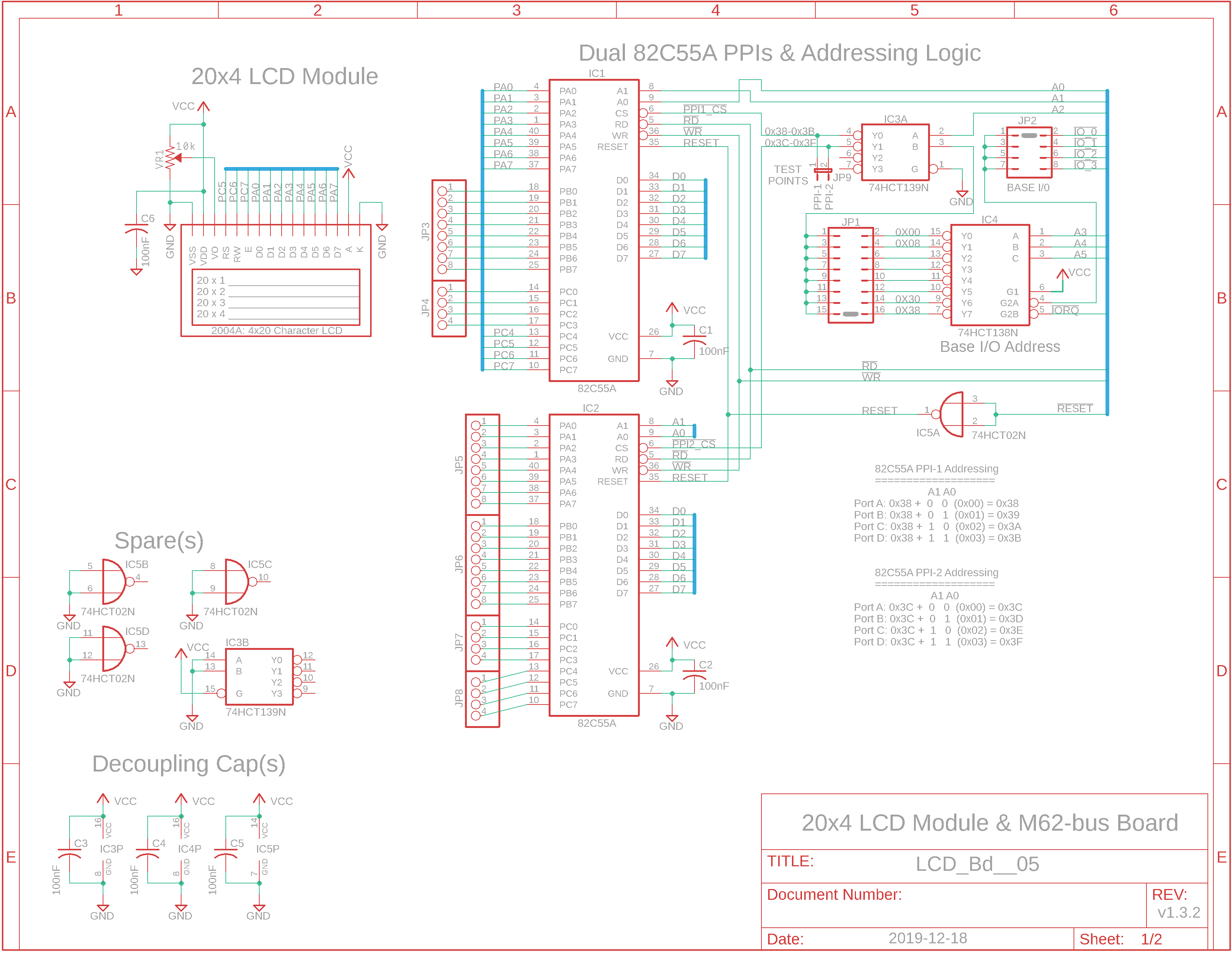
Eagle CAD: 1. 20x4 LCD module and addressing logic
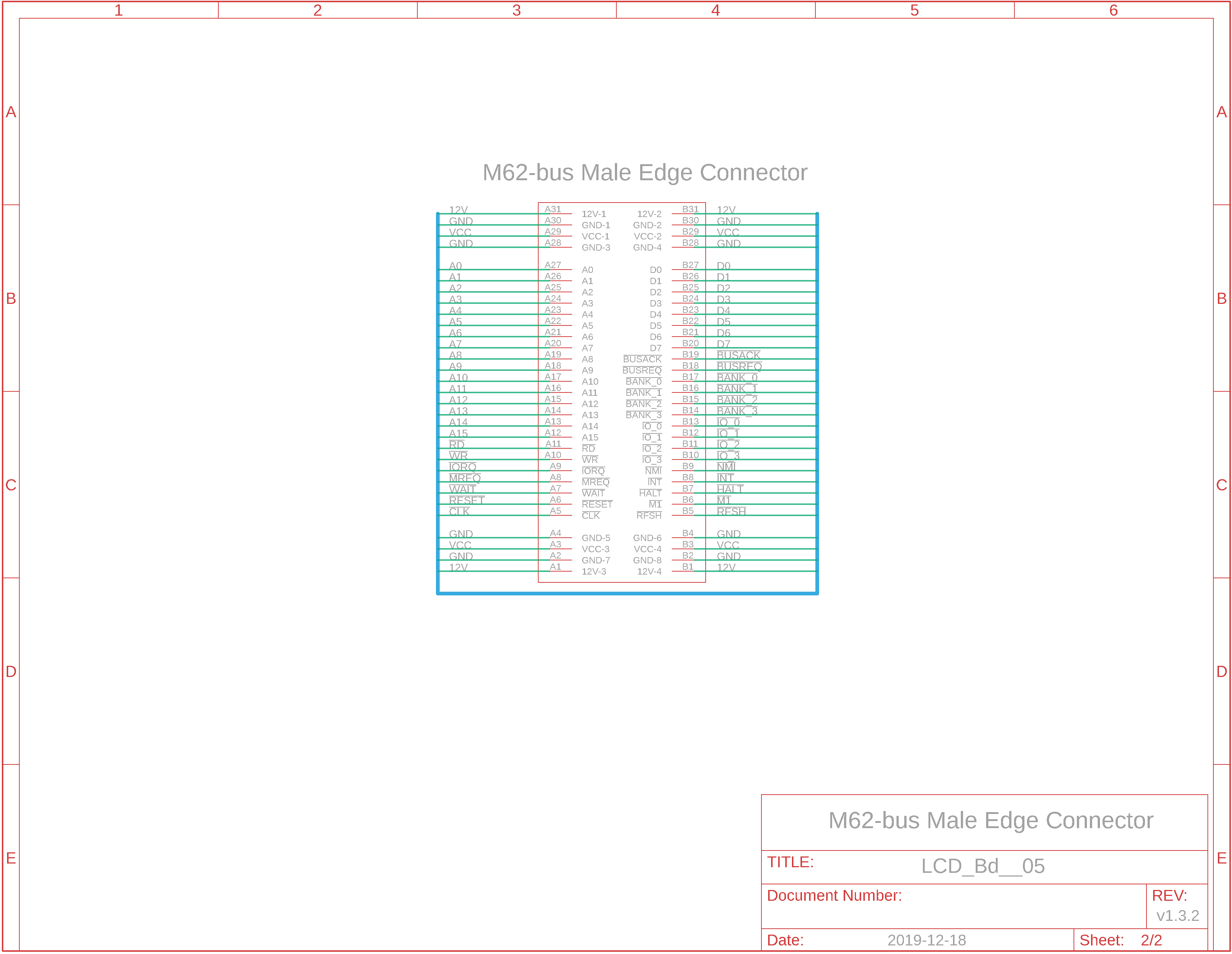
Eagle CAD: 2. M62-bus Male Edge Connector
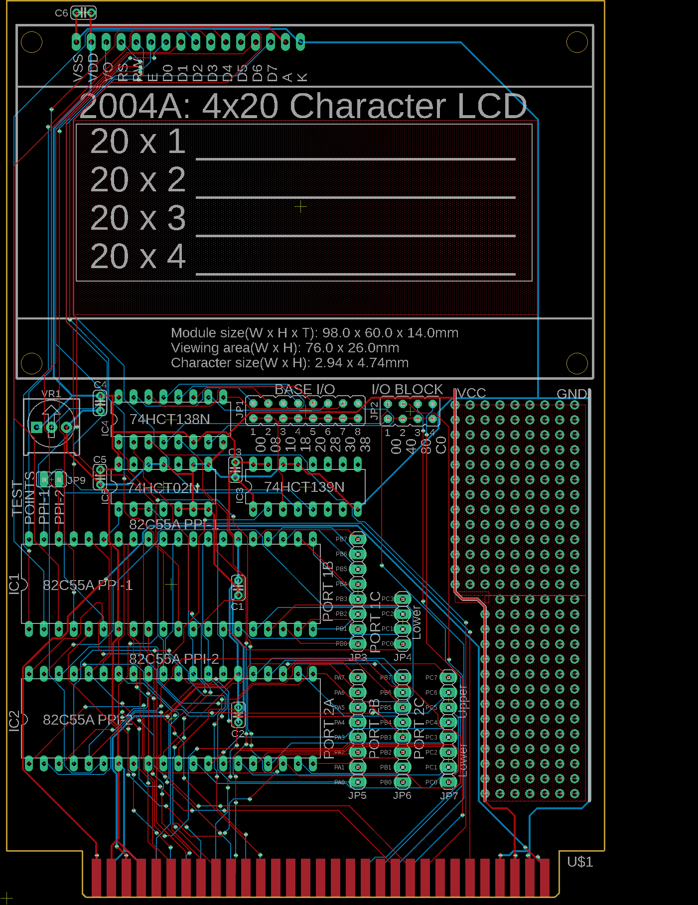
Eagle CAD: 3. A Possible PCB Layout
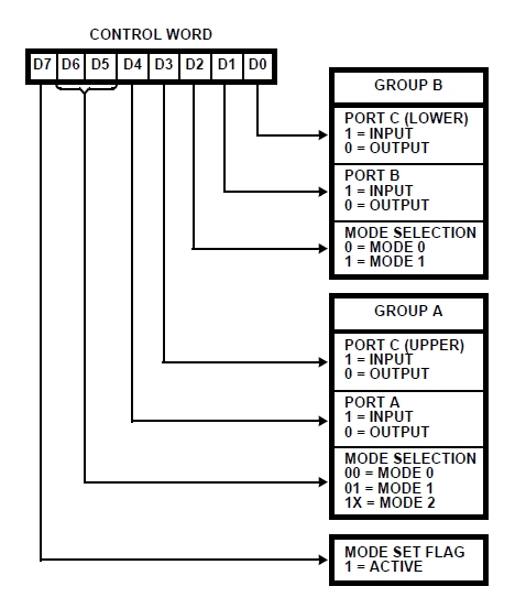
82C55A PPI Control Word Definition
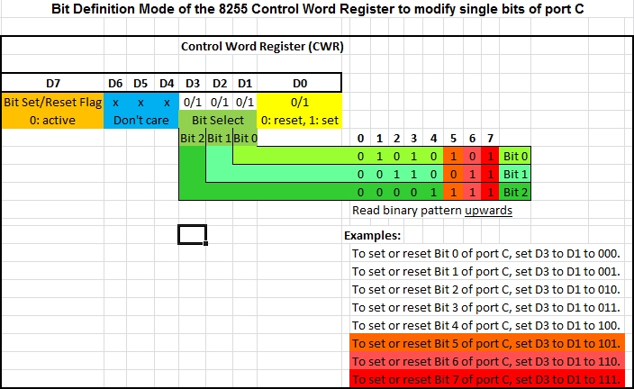
CWR: Port C Bit Modifications
Short video of user pressing "M" for Monitor
Clicking the thumbnail gif above will provide an HD video (1.31MB, .mp4 format)
(Bill of Materials) |
PLEASE NOTE: I do not sell production boards. If you would like to buy an M62 Z80 system board/parts kit, contact Peter Murray, Peter@39k.ca I simply provide you with information to build your own breadboard computer.
NOTE: 2019-12-20 The board files are being sent to China for fabrication. When they return they will be tested thoroughly. For the interim, proceed with caution.
Overview The development of this board is based on the 8255 I/O with LCD Panel and 4x4 Keypad in Circuits, except that the keypad will not be used. The 82C55A (or 8255) has three 8-bit I/O ports available. One of the ports, Port C, can be used in Mode 0 as two 4-bit ports. We will use 8-bit Port A and 4-bit Port C Upper, but not 8-bit Port B nor 4-bit Port C Lower. That will leave you 12 bits of PPI ports so you could implement a keypad function or anything else you like. Update: the latest version of the LCD board contains two PPIs so you actually have 12 + 24 bits of ports available for your development.
Addressing the devices Base I/O address via the '138 is IO_0, or $00 to $3F. Specifically, we will use I/O address $38 for the first PPI and $30 for the second PPI. If you choose to change either, you'll need to change the assembly code, of course. A0 and A1 connected to the 8255 will provide binary addresses 00 (0), 01 (1), 10 (2), and 11 (3) which will select Port A I/O, Port B I/O, Port C I/O, and the CWR (control word register), respectively. With a base address of $38 for the first PPI, the addresses will be $38, $39, $3A and $3B.
How does it work? We'll use the 8255's Port A as output to the LCD's D[0..7] data lines, and the upper half of Port C (Port C Upper) as output to the LCD's control lines RS, RW, E. As mentioned earlier, we won't use Port B nor Port C Lower. A prototyping section has been created on the side of the board for you to use these ports. We'll setup the control lines via Port C Upper, then send the LCD command or data to the data lines connected to Port A.
CWR? The 82C55A PPI is managed by the Control Word Register (CWR) and can be run in port and pin modes in Mode 0. We will not use Modes 1 nor 2 as they are overkill for an output application with no input required.
The
CWR in Port Mode:
The
CWR in Pin Mode: We wish to set or reset LCD lines RS, R/W, and E individually that are connected to Port C Upper (PC5 to PC7; we won't be using PC4).
To adjust any one of those 3 control lines to high or low requires we set 3 bits in the CWR. You may wish to examine the bottom adjacent diagram CWR: Port C Bit Modifications. As an example, to set or reset E the Enable line, we would need the following bit settings: D3=1, D2=1, and D1=1. - If we wish to set the E line, then D0 would need to be set to 1. - To reset the E line, we would need D0 to be reset to 0; we could use 0xxx1110 to reset E to 0 and 0xxx1111 to set E to 1. Thus if we send 0000 1111 (0Fh) to the CWR, we will be setting the Enable (E) pin high. For our coding, we could create an assembler EQU of "ENABLE" using 0x0F; "DISABLE" would be 0x0E.
Three LCD Control lines to be controlled by the PPI: 8255 line PC5 is connected to LCD RS line (command=low, data=high) 8255 line PC6 is connected to LCD R/W line (Read=high, Write=low). 8255 line PC7 is connected to LCD E line (Enable is pulsed high then low).
8255 Control Word Register (CWR) Config Values: To
initially configure the 8255 to use Port A and Port C Upper (Port B
and Port C Lower will be outputs to avoid needing to attach pulldown resistors).
portMode Mode0 portA-Input portC-UpperOutput
portB-Output portC-LowerOutput Binary Hex
Test Program Run 8255LCD_02.bin at $4000. I have added this to the BIOS v1.2.4 dated 2019-11-22. The LCD program will test better when the PCBs return from fabrication.
I see the schematics. Where is the Bill of Materials parts list? The BOM is at the bottom of the adjacent panel.
How big is the Serial Interface board and what will the printed circuit board look like? The PCB measures 100mm x 150mm (4"W x 6"H).
Note: M62 Bus is copyrighted by Peter Murray of Murray Electronics, http://www.39k.ca |
![]()
Tags: Z80 SBC, 82C55A UART