|
Part 1: CPU, ROM, RAM Wiring |
|
|
Read_Data_01 Read_Data_02
(Click on Images to Enlarge)
BB_01 BB_02 BB_03
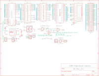
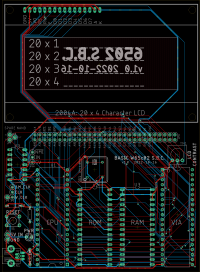
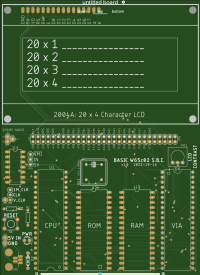
Eagle: Schematic Eagle: Board Layout Gerber Viewer: PCB Layout
|
THE HARDWARE DEVELOPMENT STORY SO FAR...
Initial schematic design was via Eagle CAD and the circuit was breadboarded to test it. I highly recommend reviewing Ben Eater's Build a 65c02-based computer from scratch nine videos series on YouTube prior to starting this build.
Build and Testing Materials After many years of reliable service my personal choices for breadboard (BB) and jumper wire are: - BB: https://www.radioshack.com/products/universal-solderless-breadboard - Machine Pin Jumper Wires: https://www.circuittest.com/mb-940-flexible-wire-jumpers.html
In The Beginning I was having trouble getting the Arduino Serial Monitor to output reasonable data - everything (addresses and data) was "backwards". I reversed the pin order in the Arduino code so that pin 52 was listed first and pin 22 was listed last in the ADDR[] array and the same for the Data[] array: pin 53 was listed first and pin 39 was listed last. This fixed the issue as can be seen in screenshot Read_Data 02 (click to expand): after the first 7 lines (CPU's built-in boot sequence) we can see the read for Reset addresses FFFC and FFFD to find the program address EAEA. This EA data was created by wiring 1K resistors for D0 to D7 to GND for a Low or to VCC for a High. They were wired as LHLHLHHH which when direction-reversed and converted to binary is 1110 1010 or 0xEA in hex. That is why the first read after FFFC and FFFD is to address EAEA. The ROM code that will be used later on is very simple and can be found in ROM_eaea.asm. For now the 8 data resistors are our "ROM". This process proved that our W65c02 CPU was working properly.
Layout and Wiring In picture BB_01 (click to enlarge) the CPU, ROM and RAM chips are laid out on the lower breadboard (BB) and 5v power is provided to each. Another breadboard is attached above the first BB which will serve as a wiring bus. Sixteen Address bus lines from the CPU are attached to the wiring bus via green wires. An Arduino UNO R3 is attached to the system at the top of the picture. 6502 address lines, A0 - A15, are attached to the UNO's D0 - D13, and A0 - A1. I used the Arduino UNO R3 until the Keye Studio Mega2560 with many more I/O pins arrived in the mail.
In picture BB_02 (click to enlarge) some of the CPU's data bus lines are attached to the wiring bus via blue wires. The CLK and R/W lines are attached to the UNO's A2 and A3 lines. Of the UNO's remaining I/O pins, this leaves only A4 and A5 to serve the 8 data lines, D0 to D7. Until my Mega2560 arrives - it contains a lot more I/O pins - we can only monitor CPU data lines D0 and D1 with UNO's A4 and A5, respectively.
We'll need to put instructions in the ROM to get it to work so we'll wire in the ROM's address and data bus lines to the wiring bus.
In picture BB_03 (click to enlarge), both the ROM and RAM are wired in. As per the schematic, a NAND logic chip (74HCT00) is added and the logic is wired up, too.
Power Sources Power is from a 2-wire 5v source. The schematic/board layout show both the 2-wire and a 5v miniUSB connector; only one or the other should be used. The top rail of the upper BB is split in half by Radio Shack. I used a low-forwarding-voltage diode (1N5817-T) to bridge the gap between halves and act as a polarity check in case you plug in the two wires incorrectly.
Adjacent are the Eagle CAD schematic and board layout as well as the PCB Layout for our circuit so far.
A simple, variable (1Hz to 100Hz) CPU Clock for the system can be found here. A more feature-rich version with single-stepping and which could include a 1MHz oscillator can be found here.
|


