|
CIRCUIT 1-4: Memory |
| Name | Circuit Schematics (click to enlarge) | Info | |||||||||||||||||||||||||
|
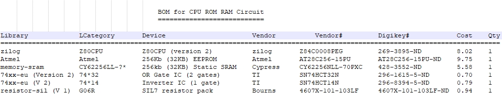
Memory: EEPROM & SRAM
(Bill of Materials)
|
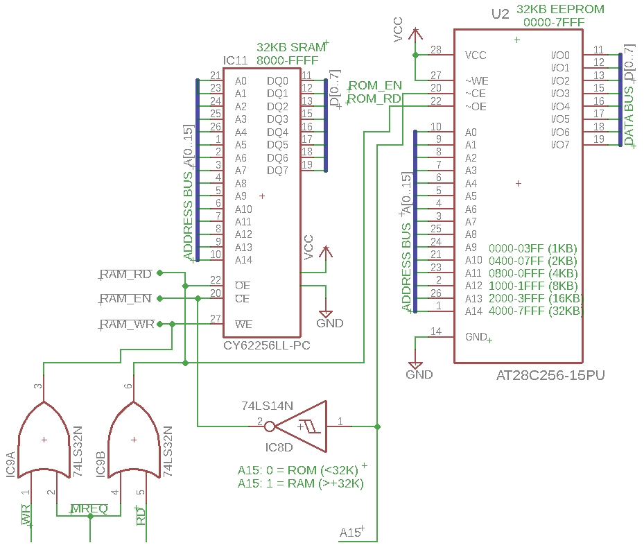
Eagle CAD: ROM, RAM and Glue Logic
Addressing Logic
|
This circuit, via the addressing "glue logic"
shown, will connect ROM (EEPROM) and RAM
(SRAM) to our Z80 CPU. The ROM on the right will occupy the lower 32KB (0x0000 to 0x7FFF) and the RAM on the left will occupy the upper 32KB (0x8000 to 0xFFFF) of our 64KB address space. Positive assertion of the A15 address line is for addresses of 0x8000 and above. As long as the addresses are below 0x8000, the EEPROM will be used (ROM_EN) because the 74HCT14 inverts the 0 signal on A15 to a 1, thus disabling the RAM_EN line to the SRAM. When address line A15 is asserted high, the RAM is used and the ROM is not. When both MREQ and RD are enabled during an M1 instruction fetch, either the ROM or RAM will be read depending upon the state of the A15 address line. Note that when MREQ is asserted, RD or WR is also asserted during the first byte read of the instruction. If the instruction is composed of multiple bytes, then an additional MREQ and RD/WR pairing is asserted for each byte. In our RAM test program listing, Block_Fill.lst, the first instruction is ``LD HL, 8000h`` which is composed of 3 bytes: 21 00 80. We expect the initial M1 and MR/RD, followed by two more MR/RD assertions for the remaining 2 bytes. When both MREQ and WR are enabled during an M1 instruction fetch, only the RAM will be written to if A15 is high; this cannot happen if A15 is low because we tied the ROM`s WE line to a logic high to ensure the ROM contents are not accidentally changed.
Test Your Circuit Visit CPU EEPROM Test and CPU SRAM Test to test your circuits. They contain useful info and video demos.
Z80 Assembly Language Programming Visit Z80 Programming IV to learn how the Assembly code works for this circuit. |